Support Forum
How to extract the netlist from the layout
User
Tuesday 14th February 2023 How to extract the netlist from the layout
Tuesday 14th February 2023 How to extract the netlist from the layout
Jürgen
LayoutEditorFull
Tuesday 14th February 2023
Attachments:
(only for registered users)
Screenshot_20230214_161721.png
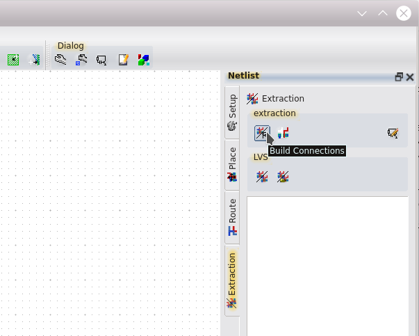
In the netlist window is a tab *extraction*. The button *build connections* will create the connections and with the *edit* button right of it you can view the netlist:  The LayoutEditor does not include a device detection. So for example in case you draw a transistor by hand it will not be detected. But if you use the SchematicDrivenLayout the created devices are connected and will be detected. Also the connectivity between subcells will be detected. A correct layer setup with connecting and via layers will be required in any case the use this feature.
LayoutEditorFull
Tuesday 14th February 2023
Attachments:
(only for registered users)
Screenshot_20230214_161721.png
In the netlist window is a tab *extraction*. The button *build connections* will create the connections and with the *edit* button right of it you can view the netlist:  The LayoutEditor does not include a device detection. So for example in case you draw a transistor by hand it will not be detected. But if you use the SchematicDrivenLayout the created devices are connected and will be detected. Also the connectivity between subcells will be detected. A correct layer setup with connecting and via layers will be required in any case the use this feature.
User
Wednesday 15th February 2023 Thank you very much for your answer! But the current situation is: the layout of the device is entirely drawn by my own hand, how can I make the software recognize that I this layout represents a certain device, in other words how can I correspond my drawn layout to a device?
Wednesday 15th February 2023 Thank you very much for your answer! But the current situation is: the layout of the device is entirely drawn by my own hand, how can I make the software recognize that I this layout represents a certain device, in other words how can I correspond my drawn layout to a device?
Jürgen
LayoutEditorFull
Wednesday 15th February 2023
Attachments:
(only for registered users)
Screenshot_20230215_105645.png
Screenshot_20230215_105708.png
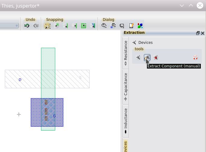
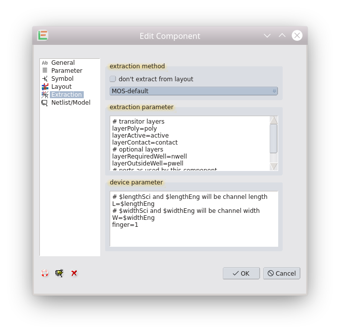
In this case you will need in the first step a corresponding device in the SchematicEditor. It must contain the information on the netlist display of this device. Once this step is done you are able to manual extract the device from the layout. This is done with the extraction tools window on the tab *Devices*. Click on *manual extraction* and choose the device type you want to extract. Afterward you can set the connections of this device in the layout. The layer of the set connection locations must be on a technology layer (=ether connector or via in the LayerManager). Once this step is done you can extract the netlist in the same way as described before.  Some kind of automatic extraction is also possible. In this case you need also complete the *extraction* part of the device in the SchematicEditor. This section will get visible after pressing the little + in the lower left of the *edit component* dialog: 
LayoutEditorFull
Wednesday 15th February 2023
Attachments:
(only for registered users)
Screenshot_20230215_105645.png
Screenshot_20230215_105708.png
In this case you will need in the first step a corresponding device in the SchematicEditor. It must contain the information on the netlist display of this device. Once this step is done you are able to manual extract the device from the layout. This is done with the extraction tools window on the tab *Devices*. Click on *manual extraction* and choose the device type you want to extract. Afterward you can set the connections of this device in the layout. The layer of the set connection locations must be on a technology layer (=ether connector or via in the LayerManager). Once this step is done you can extract the netlist in the same way as described before.  Some kind of automatic extraction is also possible. In this case you need also complete the *extraction* part of the device in the SchematicEditor. This section will get visible after pressing the little + in the lower left of the *edit component* dialog: 
User
Monday 20th February 2023
Attachments:
(only for registered users)
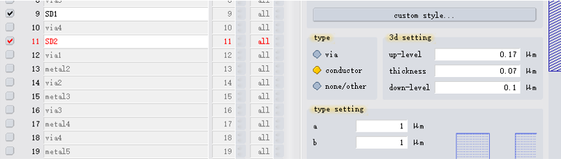
figure1.png
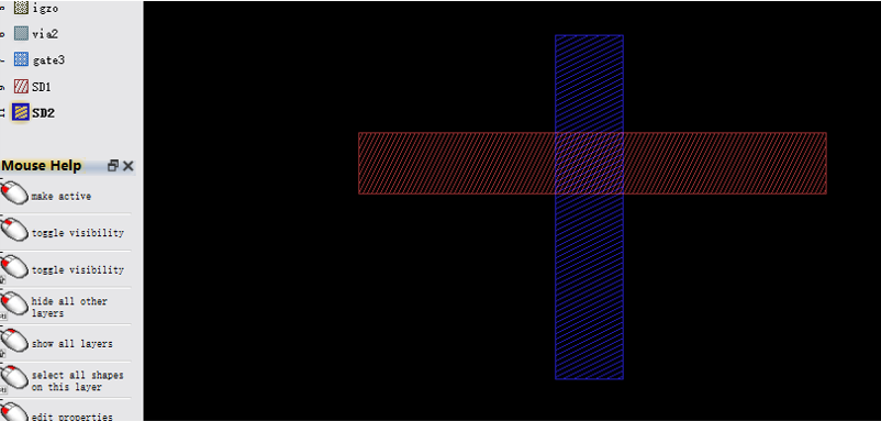
figure2.png
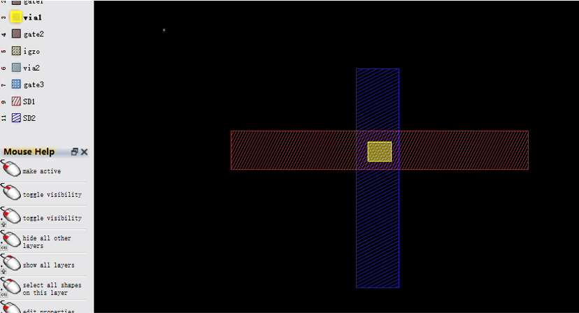
figure3.png

figure4.png
Thank you very much for your answer. Based on your answer I have been able to extract the netlist information from the layout. Thank you very much! However, I encountered a new problem, and I wanted to give up for a while, but finally had no choice but to ask for your help again. As shown in figure 1, I have defined two layers SD1 and SD2. These two layers represent two metal interconnect layers respectively.These two layers belong to different layers in the foundry. Therefore, even if I draw a layout in the LayoutEditor where SD1 and SD2 intersect (as shown in figure 2), they do not make any electrical connection, and only when I place a via (as shown in figure 3), the electrical connection between SD1 and SD2 occurs. But when I change the type of SD1 and SD2 to conductor (as shown figure 4), the software defaults to the electrical connection between the two layers, even if I do not place a via. So the netlist extracted from the layout is always wrong. My question is, how can I make the software understand my intention and generate electrical connections according to my connection rules.
Monday 20th February 2023
Attachments:
(only for registered users)
figure1.png
figure2.png
figure3.png
figure4.png
Thank you very much for your answer. Based on your answer I have been able to extract the netlist information from the layout. Thank you very much! However, I encountered a new problem, and I wanted to give up for a while, but finally had no choice but to ask for your help again. As shown in figure 1, I have defined two layers SD1 and SD2. These two layers represent two metal interconnect layers respectively.These two layers belong to different layers in the foundry. Therefore, even if I draw a layout in the LayoutEditor where SD1 and SD2 intersect (as shown in figure 2), they do not make any electrical connection, and only when I place a via (as shown in figure 3), the electrical connection between SD1 and SD2 occurs. But when I change the type of SD1 and SD2 to conductor (as shown figure 4), the software defaults to the electrical connection between the two layers, even if I do not place a via. So the netlist extracted from the layout is always wrong. My question is, how can I make the software understand my intention and generate electrical connections according to my connection rules.
Jürgen
LayoutEditorFull
Monday 20th February 2023 No problem to ask question. This forum is made for it ;-) To your question: that is all a matter of layer setup. The conductivity between layer is extracted from the layer setup. If you have setup two conductive layers and a via layer with a 3d level between the two conductive layers, this via layer is supposed to be the via layer between these two conductive layer. However, if there is no via layer, it is assumed that the two conduction layers connect. So you just need to define an empty via layer between the two layer and everything should be fine.
User
Monday 20th February 2023
Monday 20th February 2023
User
Monday 20th February 2023 You are really kind and your help is so important to me. I have some more questions. 1. what does empty via mean and how to set it 2. how to set the via type to make the via conductive, so that I can connect two different conductive layers through the via Your answer really means a lot to me, I don't even know how to express my gratitude!
Monday 20th February 2023 You are really kind and your help is so important to me. I have some more questions. 1. what does empty via mean and how to set it 2. how to set the via type to make the via conductive, so that I can connect two different conductive layers through the via Your answer really means a lot to me, I don't even know how to express my gratitude!
Jürgen
LayoutEditorFull
Monday 20th February 2023
Attachments:
(only for registered users)
Screenshot_20230220_163043.png
Screenshot_20230220_163239.png
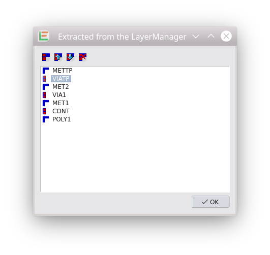
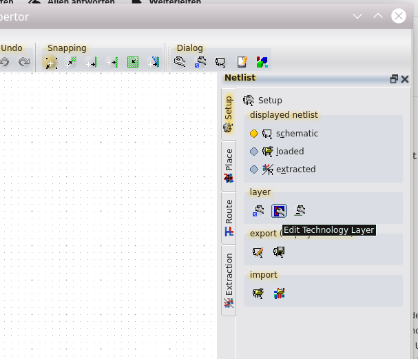
To understand the system behind it, it can be helpful to start with a ready setup. For example you will find an layer setup with conductive and via layer under mainmenu/utilities/technology/openCellLibrary/layer_setup. Once called that menu item and can go to the LayerManager and click on the different layers. Some are set as conductive layer and some as via layers. Right to the layer type you will find the 3d settings as well as a 3d side view. These setting are important to the layer order. So the 3d level of via3 is between met3 and met4. As the result via3 is the via between met3 and met4. You can verify the layer order via the feature *Edit Technology Layer* The feature is loacted in the netlist tools under setup layer.  
LayoutEditorFull
Monday 20th February 2023
Attachments:
(only for registered users)
Screenshot_20230220_163043.png
Screenshot_20230220_163239.png
To understand the system behind it, it can be helpful to start with a ready setup. For example you will find an layer setup with conductive and via layer under mainmenu/utilities/technology/openCellLibrary/layer_setup. Once called that menu item and can go to the LayerManager and click on the different layers. Some are set as conductive layer and some as via layers. Right to the layer type you will find the 3d settings as well as a 3d side view. These setting are important to the layer order. So the 3d level of via3 is between met3 and met4. As the result via3 is the via between met3 and met4. You can verify the layer order via the feature *Edit Technology Layer* The feature is loacted in the netlist tools under setup layer.  
User
Wednesday 22nd February 2023 Thank you very much indeed. Following your method, I have now successfully extracted the netlist from the layout. Thank you very much and if I have the chance I would really like to take you to dinner to express my gratitude.
Wednesday 22nd February 2023 Thank you very much indeed. Following your method, I have now successfully extracted the netlist from the layout. Thank you very much and if I have the chance I would really like to take you to dinner to express my gratitude.