Support Forum
Schematics, wire auto-join / "healing"
User
20190913
Friday 3rd May 2019 One issue with not having a working grid/snap is that it's very difficult to get wires added on, cleanly. I end up with many extra "solder dots" and wires that are off-point relative to the symbol port targets, little gaps that can barely be seen (and have I mentioned that "zoom in" has a maximum which is barely high enough magnification to resolve the "auto" snap-increment?). It would be nice if the wire-draw snapping recognized nearby wire ends, in the way it seems to find port-targets and snap to those. Wires should be able to have their individual vertices dragged and the end vertices should snap to other wire vertices if that's where they're being dragged.
User
20190913
Friday 3rd May 2019
Attachments:
(only for registered users)
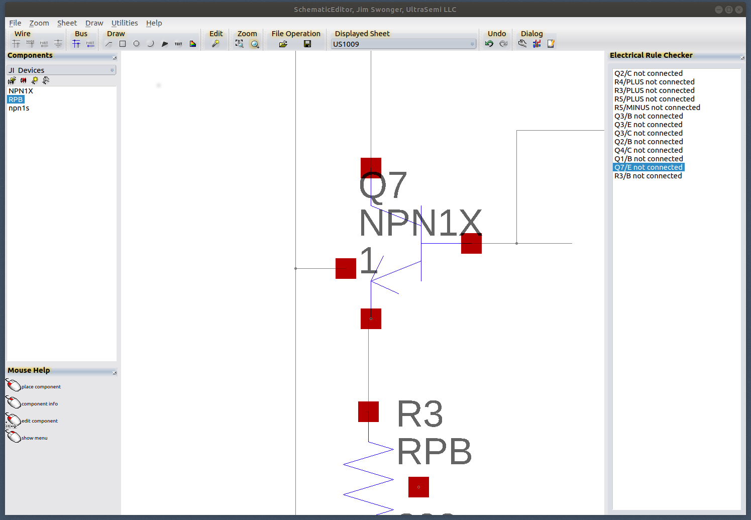
Grid_missed_target.png
Here is a snippet of a schematic in work, symbols don't place on grid and wire started from one port-target doesn't hit the other (see ERC, Q7/E)
20190913
Friday 3rd May 2019
Attachments:
(only for registered users)
Grid_missed_target.png
Here is a snippet of a schematic in work, symbols don't place on grid and wire started from one port-target doesn't hit the other (see ERC, Q7/E)
Jürgen
LayoutEditorFull
Saturday 4th May 2019 There is no grid in the schematic. Snapping is used. If you place a device next to a previous placed device it will snap in a way small wire segments as you show it in your example are avoided. However when you start a schematic at two different locations that join after some editing, small wire segments cannot be avoided. Also some symbols may use a pin placement where these small segments can not be avoided anytime.
User
20190913
Sunday 5th May 2019 I have already found that this behavior is problematic, ERC turns up many "not connected" nodes which -look- connected on the schematic but are not. Why is there no grid and grid-snap? I'm pretty sure there is a coordinate system, and sometimes instance placement snaps to it (other times, apparently not; have not figured out a pattern). Can you at least "put this on the list" of useful improvements for "someday"?? I like to draw a schematic and be done with it, not draw it and then have to chase every pin and vertex to be sure they've "caught" (and then have to delete and redraw the whole net because of no stretch funcrtion). That is not good for productivity. Can snapping be made to -always- home in on the pin target? To wire vertices or intersecting lines? Can the pin target be made an area rather than a single coordinate-pair, to make wiring more "forgiving"? And, can the maximum zoom-in be increased to let us see clearly whether the pin target is hit, or not? Failing this, can you recommend an alternate schematics tool that plays well with your layout and verification tools?
Jürgen
LayoutEditorFull
Sunday 5th May 2019 If you follow the sequence: place the devices, wire the connection your problem should not occur. When wiring it will be highlighted when you connect the wire to a device. The current created wire will be completed. Stopping a wire next to a device connection or in the middle of nowhere would require additional action to stop the current entered wire. A grid would only improve the schematic entry, if all library use this grid strictly. As there is not standard grid for schematics this grid would be different for any used library and mixing two symbols from different libraries will even cause bigger problem you have now. That is the reason no grid is used in the SchematicEditor. It will make it much possible flexible to use different libraries and avoids any special care on grids when creating new symbols.